
Etch Processes for WBG RF Devices
This Application Brief describes the reasons GaN is often selected for 5G applications, and SPTS's back-side SiC via and GaN etch processes used in the manufacturing of GaN-on-SiC RF devices.
DownloadIn February 2020, it was estimated that commercial 5G networks had been deployed in almost 400 cities across 34 countries in Asia, Europe and the Americas[1], and the global market for 5G technology (hardware, software & services) is expected to grow at a CAGR of 122% from 2020 to 2026[2].
5G communications operate at higher radio frequencies than 3G/4G technologies, where there is more free bandwidth and faster data transfer speeds. Currently 5G implementations are split into two frequency groups; (a) Frequency Range 1 (FR1) at frequencies less than 6GHz and (b) Frequency Range 2 (FR2) at >6GHz. The term “mmWave” refers to a specific part of FR2 between 24GHz and 100GHz, which have very short wavelengths. This section of the spectrum is also relatively unused, so mmWave technology greatly increases the amount of potential bandwidth available.
Because mmWave signals consists of short wavelengths, they are limited to a transmission range of only a few hundred meters in air, and they cannot penetrate through buildings and other structures. This means mmWave base stations need to be closer together than for 3G/4G/sub 6GHz 5G networks. Interest in mmWave communication is driving the need for arrays of multiple “macro” and “small cell” base stations where the RF power amplifiers and transmitters need to manage a high power density at high frequencies, in a small footprint to aid thermal dissipation. A small footprint also enables reliable coverage in an unobtrusive manner, both inside and outside buildings. These applications are ideally suited to wide bandgap materials such as GaN and GaN-on-SiC, rather than traditional Si-based LDMOS (laterally-diffused metal-oxide semiconductor) RF components, due to their higher operating voltages and faster switching capabilities.
GaN-on-SiC RF Devices
Gallium Nitride (GaN) is a wide bandgap material which has been touted as a successor to silicon-based LDMOS for many years, due to its superior electrical properties. Despite the continued evolution of LDMOS technology, GaN is finally finding its niche in high power/high frequency RF applications, with telecommunications being one of the largest[3], although it is expected that LDMOS will continue to compete with GaN in the sub 6GHz 5G arena.
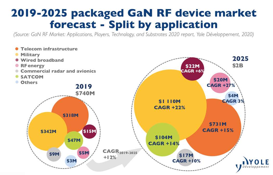
Fig. 1 Yole Développement forecasts the market for GaN-based RF devices in telecommunications infrastructure will increase to $731M by 2025 (CAGR ~15%)[3]
|
|
Si |
SiC-4H |
GaN |
|
Band Gap (eV) |
1.1 |
3.2 |
3.4 |
|
Critical Field 106V/cm |
0.3 |
3 |
3.5 |
|
Electron Mobility (cm2/V-sec) |
1450 |
900 |
2000 |
|
Electron Saturation Velocity (106 cm/sec) |
10 |
22 |
25 |
|
Thermal Conductivity (Watts/cm2 K) |
1.5 |
5 |
1.3 |
Fig. 2 Comparison of electrical properties for Si, SiC and GaN
Fig. 2 illustrates that GaN has the highest electron mobility among the three options (Si, SiC and GaN), and is therefore, theoretically, the best material for switching most efficiently at high frequencies. However, due to the difficulty and high cost of producing defect-free bulk GaN wafers, GaN is usually deposited as an epitaxial layer onto SiC (or silicon) substrates. While GaN-on-SiC epitaxy is more expensive than GaN-on-Si, the combined advantages of enhanced thermal conductivity due to the SiC substrate and a better crystal lattice match between the GaN and SiC giving higher device yields, mean that GaN-on-SiC is typically the preferred choice in RF applications where high performance, efficiency and small size are critical.
Back-side SiC Via Etch
To create an interconnect from the back-side of the SiC substrate to the active front-side GaN, it is necessary to etch a deep via through the SiC. This process is carried out on thinned wafers mounted on a carrier of SiC or sapphire. For back-side SiC via etching the etch rate is important to ensure a high throughput, and the sidewall smoothness and angle must be suitable for subsequent metal lining/plating (See Fig 3). SPTS offers their Omega® Synapse™ for deep SiC etching. This process module provides a high ion energy to achieve high etch rates. However, a highly energetic etch tends to induce micro-trenching near the sidewall, so a good selectivity to the GaN layer underneath is essential to allow sufficient over-etching to clear all the SiC from the bottom of the via, without etching the GaN layer too much. Mechanically assisted electrostatic clamping (ESC) is also available to maintain consistent wafer temperature and the bonding integrity with any carrier wafer.
For back-side SiC via etching the etch rate is important to ensure a high throughput, and the sidewall smoothness and angle must be suitable for subsequent metal lining/plating. SPTS offers the Omega® Synapse™ for deep SiC etching. This process module provides a high ion energy to achieve high etch rates. However, a highly energetic etch tends to induce micro-trenching near the sidewall, so a good selectivity to the GaN layer underneath is essential to allow sufficient over-etching to clear all the SiC from the bottom of the via, without etching the GaN layer too much. Mechanically assisted electrostatic clamping (ESC) is also available to maintain consistent wafer temperature and the bonding integrity with any carrier wafer.
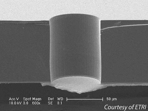
Fig. 3 Back-side via etch, 80µm deep @1.9µm/min
(Courtesy of ETRI [4])
GaN Etch
A second etch process is then required to etch through the GaN base layer. With the SPTS Synapse™ both SiC and GaN can be etched in the same process module, which reduces cost of ownership (CoO) by saving process time and capital expediture. Fig. 4 shows an etch through the GaN beneath the SiC, stopping on a thin Au layer.
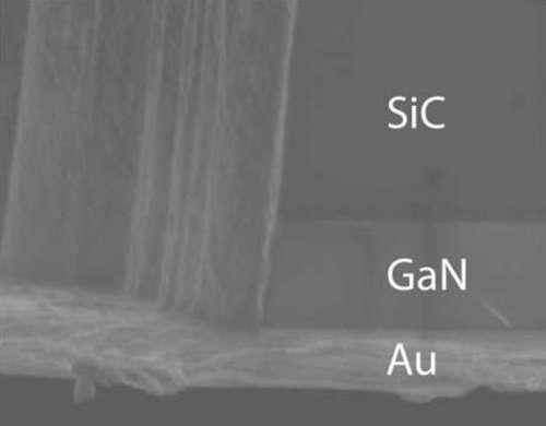
Fig. 4 GaN etch to underlying Au layer
For further information on SPTS’s Omega® Synapse™ for SiC/GaN etching, contact us.
[1] https://www.viavisolutions.com/en-us/literature/state-5g-deployments-2020-poster-chart-en.pdf
[2] https://reports.valuates.com/market-reports/ALLI-Manu-1C7/5g-technology-market
[3] “GaN RF Market: Applications, Players, Technology and Substrates 2020 Report”, Yole Développement (May 2020)
[4] “Backside Via Process with Defect Free Sidewalls for GaN MMIC Applications”, Kyu Jun Cho etc al Proc. CS Mantech 2017
Information on this page contains forward looking information. For more information, click here
The link you have selected is located on another server. Neither SPTS Ltd. nor any of its subsidiaries endorses this web site, its sponsor, or any of the information, policies, activities, products, or services offered on the site or by any advertiser on the site. By clicking on the OK button below, you agree and acknowledge the foregoing and will be directed to the selected site.